Nano Ceramic: What It Is and Why It Matters in 2026

This material is one of the most transformative materials of the modern era, yet most people encounter it daily without knowing it exists. From the coating protecting your car’s paint to the components inside your smartphone, from medical implants to aerospace shielding, this advanced material is quietly powering the technology that defines modern life.
- What Is Nano Ceramic?
- What Is Nanotechnology? The Science That Makes It Possible
- Applications Across Industries
- Nano Ceramic Market Size and Growth
- Nano-Ceramic vs Traditional Ceramic: Key Differences
- Advantages and Limitations
- The Future of This Technology
- Conclusion
- Frequently Asked Questions (FAQ)
In this guide, you will find everything: what it is, the science behind Nano ceramic how nanotechnology makes it possible, its applications across industries, its advantages over traditional materials, market growth data, and what the future holds for this remarkable material. Whether you are a student, a professional, or simply curious about the technologies shaping your world, this is your complete resource.
What Is Nano Ceramic?
Nano ceramic refers to ceramic materials engineered at the nanoscale, meaning their grain sizes or structural features measure between 1 and 100 nanometers. To put that in perspective, a single human hair is approximately 80,000 to 100,000 nanometers wide. At the nano scale, materials behave in fundamentally different ways than their bulk counterparts.
Traditional ceramics, the kind used in pottery, tiles, and basic industrial applications, have grain structures measured in micrometers. When those same ceramic compounds are reduced to the nanoscale, the resulting material exhibits dramatically enhanced properties:
- Superior hardness: These materials are among the hardest known to science
- Exceptional thermal resistance: They maintain structural integrity at temperatures that would destroy metals and polymers
- Outstanding chemical stability: resistant to corrosion, oxidation, and chemical attack
- Enhanced optical properties: Some formulations are transparent or have tunable light transmission
- Improved biocompatibility, making them suitable for medical implants and drug delivery
These properties emerge from a combination of quantum size effects and the enormous specific surface area that nanoscale structures create, giving these materials their unique performance profile.
What Is Nanotechnology? The Science That Makes It Possible
To fully understand What Is Nanotechnology it helps to understand what nanotechnology is at its core. Nanotechnology is the science of designing, manufacturing, and applying materials and devices at the atomic and molecular scale, specifically in the 1 to 100 nanometer range.
At this scale, the laws of classical physics give way to quantum mechanical effects. Materials that are brittle at the macro scale become flexible. Compounds that are opaque become transparent. Substances that conduct heat poorly become excellent thermal conductors.
Nanotechnology enables the creation of these materials through precision manufacturing processes including:
- Sol-Gel Processing: A chemical process that converts a solution into a solid gel, allowing precise control of grain size at the nanoscale. Widely used for producing such coatings and powders.
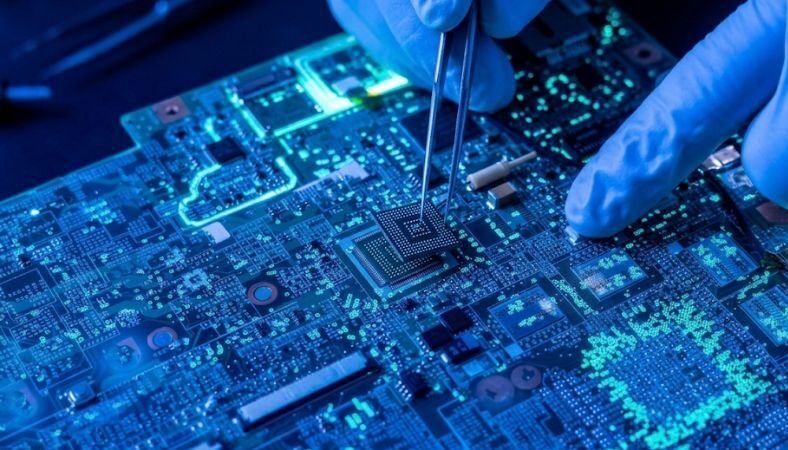
- Chemical Vapor Deposition (CVD): A process that deposits thin nanoscale ceramic films onto surfaces by chemical reaction of vapor-phase precursors. Used extensively in electronics and semiconductor manufacturing.
- Hydrothermal Synthesis: High-pressure, high-temperature water-based reactions that produce nanoscale ceramic powders with tightly controlled particle sizes and compositions.
- Spark Plasma Sintering (SPS): A rapid sintering technique that densifies these powders while preserving their nano-scale grain structure critical for maintaining the performance properties that make these materials valuable.
Understanding nanotechnology clarifies why this material performs so differently from conventional ceramics; it is not just a size difference, it is a fundamentally different material behavior at the quantum level.
Applications Across Industries
The versatility of this material is extraordinary. Here is a complete breakdown of where it is actively deployed in 2026:
Automotive Industry
The automotive sector is one of the largest consumers of this technology. Applications include:
- Paint protection coatings: These coatings bond to vehicle paint at the molecular level, creating a hydrophobic, scratch-resistant, UV-blocking protective layer that outperforms traditional wax and polymer sealants
- Engine components such as coatings on pistons, cylinders, and exhaust systems reduce friction and improve thermal management
- EV battery module companies, including Tesla are deploying these coatings for battery thermal management and electrical insulation
- Brake systems: Brake pads made with this material offer superior heat resistance and reduced dust compared to traditional compounds
Electronics and Semiconductors
The relentless miniaturization and performance enhancement of electronic components is a primary engine for demand for this material. The global demand for multilayer ceramic capacitors (MLCCs), a critical component in virtually all modern electronics, is a key indicator of the sector’s growth.
Specific applications include:
- MLCCs (Multilayer Ceramic Capacitors): These dielectric layers enable smaller, higher-capacity capacitors in smartphones, laptops, and electric vehicles
- Semiconductor substrates these materials provide the thermal and electrical properties required by advanced chip packaging
- Display technology such coatings improve scratch resistance and optical clarity on screens
Healthcare and Biomedical
Biomedical applications in drug delivery and tissue engineering are driving adoption of ceramic nanoparticles, with the market expanding rapidly as FDA nanomaterial guidance tightens purity and characterization requirements.
Medical applications include the following:
- Dental restorations composites made from this material are used in tooth-colored fillings and crowns, combining aesthetics with durability
- Orthopedic implants: Such coatings on titanium implants improve osseointegration, the bonding of implant to the bone.
- Drug delivery systems ceramic nanoparticles can encapsulate drugs and release them at targeted locations in the body
- Surgical tools such coatings reduce friction and improve the longevity of surgical instruments
Aerospace and Defense
Defense applications benefit from these materials in armor plating and missile shielding, where material integrity under ballistic impact is paramount.
- Thermal barrier coatings on jet engine turbine blades, such coatings allow engines to operate at higher temperatures, improving efficiency
- Ballistic armor composites made from this material provide superior protection-to-weight ratios compared to conventional armor
- Spacecraft heat shields: these materials protect re-entry vehicles from extreme thermal loads
Energy Sector
- Solid-state batteries electrolytes made from this material enable safer, higher-energy-density batteries for EVs and grid storage
- Fuel cells: Such components improve the efficiency and durability of solid oxide fuel cells
- Solar panels: Such coatings improve light absorption and protect panel surfaces from environmental degradation
Nano Ceramic Market Size and Growth
The numbers behind this market tell a compelling story of a technology entering its most important growth phase.
| Market Segment | 2025 Value | 2034/2035 Projection | Growth Rate |
| Ceramic Nanopowder Market | $9.13 Billion | $15.07 Billion (2034) | 7.6% CAGR |
| Ceramic Nanoparticles Market | $6.8 Billion | $17.97 Billion (2035) | 11.4% CAGR |
| Asia Pacific Market | $3.8 Billion | $6.2 Billion (2033) | 6.4% CAGR |
| North American Market | $2.1 Billion | Growing steadily | Consistent growth |
The global ceramic nanopowder market size was valued at USD 9,132 million in 2025 and is projected to grow from USD 9,818 million in 2026 to USD 15,076 million by 2034, exhibiting a CAGR of 7.6% during the forecast period.
This growth is driven by expanding demand from electronics, electric vehicles, healthcare, and defense, all sectors that are themselves growing rapidly.
Nano-Ceramic vs Traditional Ceramic: Key Differences
Understanding what sets this material apart from conventional ceramics clarifies why it commands premium pricing and drives such strong market growth:
| Property | Traditional Ceramic | This Material |
| Grain Size | 1–100 micrometers | 1–100 nanometers |
| Hardness | High | Significantly higher |
| Toughness | Brittle | Improved fracture toughness |
| Thermal Resistance | Good | Superior |
| Optical Properties | Opaque | Can be transparent |
| Biocompatibility | Limited | Highly suitable for implants |
| Surface Area | Lower | Enormously higher |
| Manufacturing Cost | Lower | Higher (precision required) |
| Application Range | Industrial, structural | Advanced tech, medical, defense |
Advantages and Limitations
Key Advantages:
- Extreme hardness and wear resistance extend component lifespans significantly
- Exceptional thermal stability enables use in high-temperature environments impossible for metals
- Chemical inertness makes it ideal for harsh chemical environments
- Biocompatibility opens medical applications unavailable to most other materials
- Lightweight construction components made from this material weigh significantly less than metal equivalents
- Tunable properties: Grain size control allows manufacturers to engineer specific performance characteristics
Current Limitations:
- Higher manufacturing costs compared to conventional ceramics and metals
- Scaling from laboratory production to mass manufacturing remains challenging
- Long-term health and environmental impacts of these particles require ongoing research
- Brittleness, while improved over traditional ceramics, remains a consideration in structural applications
- Regulatory frameworks for nanomaterials are still evolving in many jurisdictions
The Future of This Technology
The future prospects of these materials are promising, with potential applications in emerging fields such as energy harvesting and storage, biomedical engineering, and advanced electronics.
Key developments expected through 2030:
- Additive manufacturing integration 3D printing with these materials is enabling complex geometries previously impossible to manufacture
- Flexible formulations: New compositions combining this material with polymer matrices create flexible components for wearable electronics and sensors
- AI-driven materials design: Machine learning is accelerating the discovery of new compositions with specific engineered properties
- Green manufacturing sustainable synthesis routes are reducing the environmental footprint of its production
- Wider EV adoption: As electric vehicle production scales globally, demand for this material in batteries, motors, and thermal management will grow substantially
Conclusion
Nano ceramic is not a future technology; it is a present-day material already embedded in the products, vehicles, medical devices, and infrastructure that define modern life. Its combination of extraordinary hardness, thermal resistance, chemical stability, and biocompatibility makes it one of the most versatile and valuable materials available to engineers and scientists today.
The key takeaways:
- These materials have grain sizes of 1–100 nanometers, fundamentally different from conventional ceramics
- Nanotechnology enables their creation through precision manufacturing processes including CVD, sol-gel, and spark plasma sintering
- Applications span automotive, electronics, healthcare, aerospace, and energy sectors
- The global market is projected to reach $15–18 billion by 2034–2035, growing at 7–11% annually
- Future developments in additive manufacturing, flexible ceramics, and EV applications will drive the next growth phase
Frequently Asked Questions (FAQ)
What is nano ceramic used for?
It is used in car coatings, medical implants, electronics, and aerospace shielding. Its hardness and heat resistance make it ideal for demanding applications.
Is this type of coating worth it for cars?
Yes, it bonds ata molecular level,l providing scratch resistance, UVprotection,n and durability. It lasts 2 to 5 years, unlike traditional wax.
How is it different from regular ceramic?
It has grain sizes of 1–100 nanometers, making it harder, tougher, and more versatile. Traditional ceramics have much larger grain sizes with limited properties.
Is it safe for medical use?
Yes, it is widely used in dental and orthopedic implants due to excellent biocompatibility. It passes rigorous safety testing before any medical application.
What is the market worth in 2026?
The market is valued at approximately $9.8 billion in 2026. It is projected to reach $15–18 billion by 2034.